4.2.2 - Two Sets of Zener + Diode in Parallelclick here!
So far we have seen the basic application of diodes as an AC voltage rectifier. However, there are many special
applications where diodes occupy a prominent place. In this chapter we will look at a series of circuits where diodes can be
employees with great performance.
In many circuits containing several diodes, it is necessary to know the conduction state of these diodes.
There are several techniques for finding out which diode is in cut-off or conduction.
One of the most widely used techniques is to assume that some diodes are conducting and others are cutting. The
Figure 65-01 presents a typical circuit employing two diodes.
Figure 65-01
The basic idea is to find out what the voltage value will be V0. In this case, in principle, inspection is easy
notice that the D1 diode is cut-off while the D2 diode is conducting. Just for a matter of
didactics, be D2 in cut-off and D1 in conducting state. Assuming this premise, what will be the
answer obtained? Here the value of VD = 0.7 V will be adopted when the diode is in conduction state.
If D1 is conducting so we are known that the voltage Va = - 0.7 V.
Note that in this case there has already been an incongruity with the premise, because with this value of Va necessarily diode
D2 is conducting. Therefore, it is concluded that this premise does not satisfy the solution of the problem.
Therefore, a new premise should be investigated by adopting D1 in cut-off while the
D2 diode in conduction . To solve this problem, let's rely on Figure 65-02.
In this case, we can calculate the current that circulates through the circuit, knowing that by
D1 no electric current will circulate. Then, we have that I = I1 = Io.
So the mesh equation will be:
-10 + 5k I + 0.7 + 1k I -10 =0
Working algebraically the equation, we get:
I = 19.3 / 6k = 3.22 mA
Therefore, the output voltage V0 will be:
V0 = -10 + 1k x 3.2 mA = - 6.78 volts
And if V0 = - 6.78 V, then Va = - 6.08 V. Therefore, this premise does
not satisfy the solution of the problem either, because with Va = - 6.08 V it means that
D1 is conducting.
Figure 65-02
Therefore, we must consider the alternative in which D1 and
D2 are conducting. If D1 is conducting, then Va = - 0.7 V.
In Figure 65-02 we show the circuit with the indication of currents. Knowing Va we can calculate
V0, just add the voltage drop over D2. Then:
V0 = - 1.4 volts
To complete the solution of the problem we will calculate the currents in the circuit.
I1 = (10 - (-0.7)) / 5k = 2.14 mA
I0 = (10 - 1.4) / 1k = 8.6 mA
From the circuit, we are known that I0 = I1 + ID. So:
ID = I0 - I1 = 6.46 mA
Therefore, after establishing several premises it was found that the only viable one was the last one. The other two previous ones conflicted.
This example served to illustrate one of the most commonly used techniques for solving this type of problem. On the Problems tab there are several proposed circuits with their respective solutions.
In many applications there is a need to limit the waveform to a certain voltage or current level, passing only the signal that occurs above or below a predetermined value. This feature is used in applications that include the
limitation of excessive amplitudes, formation of certain types of waveforms and also in the control of the power delivered to a
charge.
The diodes can be combined with resistors to perform the function of a limiter.
Circuit transfer characteristics are obtained using the voltage drop circuit model
diode constant (VD = 0.7 V). However, a smooth transition between the linear and saturation regions of the transfer characteristics is assumed.
We can have a simple limiter when only one of the waveform polarities is limited. Or, a double limiter, when both the positive and negative part of the waveform are limited.
First, let's study the simple type limiter and analyze its behavior when subjected to a sine wave.
Figure 65-03Figure 65-04
In the Figure 65-03, we present the scheme of a simple limiter composed of a diode and a resistor. When the voltage
Vi (by assumption a sine wave) has a positive peak and reaches a value of 0.7 V, the D diode
goes into conduction not allowing the voltage Vo exceed this value. For the negative cycle of Vi,
the diode is cut-off and in Vo input voltage appears without any change.
In the Figure 65-04, we present the graph of the circuit transfer characteristic. Note that for negative values of
Vi we have a linear response to the input voltage. For positive values, the response is not linear, setting
the output voltage to 0.7 V. Of course we can obtain multiple voltages of 0.7 V at the output, provided that
diodes are added in series.
Figure 65-05
See Figure 65-05 for the representation of a sine waveform at the input and the limited wave at the positive peak appearing at the output. Note that a voltage with 1 volt peak was used at the input. If the input peak voltage is less than
0.7 V, so there will be no limiting as the input voltage does not exceed the diode conduction voltage. Therefore, we can use this circuit whenever we need to protect the input of some circuit against overvoltage.
In practice, there are situations where there is a need to limit the output to a voltage other than of 0.7V. In this case, it is possible to add a voltage source in series with the diode to move the actuation point of the diode.
Figure 65-06
In the Figure 65-06 see an example circuit for this case. We show the modified circuit where a voltage
source Vd, this value, which is how much we want to move the limiting point, was added in series
with the diode. So the point of limiting will be given by Vd + 0.7. Note that if the peak value of
the input voltage Vi not reach the value Vd + 0.7, the sine wave does not change any output.
Of course if we want a limitation only on the negative peak, then we must invert the position of the diode
and the source Vd in the circuit above. With this, we will be causing a limitation of the negative
part of the sine wave, while not changing the positive peak.
The double limiter acts on both positive and negative parts of the sinusoid. The most common circuit for obtaining
this limitation is that shown in Figure 65-07. They are two diodes connected in parallel and in the arrangement called counter phase.
The diode D1 acts on the positive part of the sinusoid, while D2 acts on the negative part.
Figure 65-08
In the Figure 65-08 we present the graph of the transfer characteristic of the double limiter circuit.
Note that the output voltage is limited between the voltages + VD and - VD. Thus,
even if the input voltage is significantly increased, the output voltage will remain between the two values above.
Of course, in the double limiter the same concept applies as adding a voltage source in series with the diode to shift
the wave limit point at the output. Making the voltage sources with different values, we will have limiting points
different, that is, at the output we will get an asymmetric waveform.
Figure 65-09
In Figure 65-09 we can see a double limiting circuit with voltage sources connected in series with the diodes.
This causes a shift of the limit point at the circuit output. Note that the two sets are in parallel.
If VD1 > VD2 or VD1 < VD2, let's get an asymmetric waveform on the output.
The graph of the circuit transfer characteristic is similar to that of Figure 65-08 . Of course, for the positive
part of the sinusoid, we must replace the value VD by VD1 + VD. And for the
negative sinusoid cycle, we must replace - VD by - (VD2 + VD ). To eliminate
voltage sources in series with the diodes, we can use zener diodes. We will study these settings in the next item.
One way to avoid using diode voltage sources in order to achieve a certain level of limitation is to use
the zener diode. Since we have zener diodes with various operating voltages, we can choose the one that best suits our needs.
In Figure 65-10 we show the circuit using zener as a voltage limiter.
Note that in this case, the zener will not allow at the output the positive peak of the input signal to exceed the working
voltage of the zener. Thus, at the output we will have a limited signal at the positive peak with a maximum voltage equal to Vz.
Figure 65-11
However, this circuit presents a problem when the input voltage passes to the negative part of the sine.
This is due to the fact that in the negative part the zener diode will behave like a common diode, that is,
the negative peak at the output will be limited to 0.7 V . See Figure 65-11 what the output
voltage would look like using a zener with an operating voltage of the order of 6.2 volts and the
input voltage being given by Vi = 10 sin ω t. Note that the positive part of the
sinusoid is limited by 6.2V, while the negative part is limited by - 0.7V.
Then, the maximum variation (peak to peak) of the signal at the circuit output will be equal to the difference of the two voltages, that is,
Vo = 6.2 - (- 0.7) = 6.9 volts.
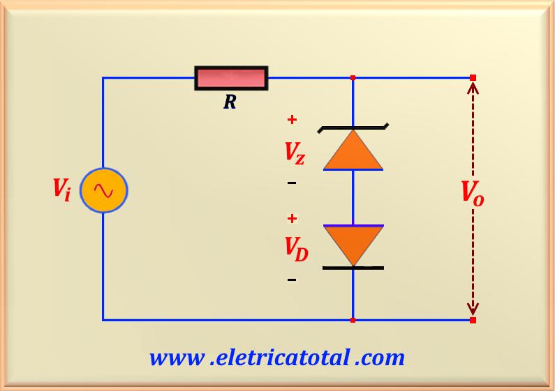
But for everything there is solution. So if we add a common diode in series with the zener, wired as shown in Figure 65-12,
in principle, we solve the problem.
Figure 65-12
We say " in principle" , because if we pay close attention to Figure 65-12 we will realize that
the output voltage of the circuit will be given by Vo = Vz + VD.
That is, in the output voltage we have to add the voltage drop in the diode, in addition to the zener voltage.
Of course this only applies to the positive part of the sinusoidal input voltage.
As soon as the input voltage is negative, the diode will enter the cut-off zone, resulting in an open circuit,
as if there were no diode and zener. Therefore, the negative part of the sinusoid appears entirely at the output
without any changes. Therefore, with the addition of a diode, we can again limit only the positive part
of the input voltage.
Of course, if we want a limiter with a cut in the negative part of the sine, just reverse the direction
of the two components.
In the Figure 65-13 we show how we can perform a double limiter. Note that the connection is in the
serial configuration, with the components in the so-called counter-phase array. In the figure, we are representing
the situation where the input voltage is in the positive part of the sine.
This way, the zener of the upper part of the figure will behave like zener, while the lower zener will behave like
a common diode. This is explicit with the indication of Vz and VD next to each zener.
So in this configuration, with the positive part of the sinusoid, we get the output voltage given by the equation
Vo = Vz + VD.
Figure 65-14
Now, in Figure 65-14 we are representing the situation where the input voltage is in the negative part of
the sinusoid. Note the inversion of the indications of Vz and VD next to each zener,
in relation to Figure 65-13. In this situation it is the lower zener that is acting as a zener, while the upper zener acts as a common diode.
So in this configuration, with the negative part of the sinusoid, we get the output voltage given by
Vo = - Vz - VD or Vo = - (Vz + VD ).
Attention
"It should be noted that the two zener need not have the same operating voltage. Obviously,
in this case the limitation will not be symmetrical. In the Problems tab we will see in more detail."
Initially, we could think of placing two zener diodes in parallel to obtain a double limiter. But if we look carefully
at the situation we will conclude that putting two zener diodes in parallel is the same as putting two common diodes in parallel.
And as we know, in this case, there will be + 0.7 V limitation on the positive part of the sinusoid and - 0.7 V
on the negative part of the sinusoid. Then we should discard this setting. However, based on the circuit shown in
Figure 65-12 showing the addition of a diode in series with zener, we have the solution to this problem.
Figure 65-15
In Figure 65-15 we show a circuit pertinent to our goals. Note that the diode + zener set highlighted
in orange will act when the input voltage is at the positive part of the sinusoid. As already mentioned, the
output voltage will be given by Vo = Vz + VD.
Of course, for the positive part of the sinusoid, the circuit highlighted in green does not work
because the diode is polarized inversely. However, when the input voltage is in the negative part of the
sinusoid, the circuit highlighted in green is acting. And of course the circuit highlighted in orange
is operating in cut-off. So for the negative part of the sinusoid the output voltage will be given
by Vo = - (Vz + VD ).
The graph of the circuit transfer characteristic is similar to that of Figure 65-08.
In this way we get a limiting circuit that acts on both sine polarities. If you are interested in working with different limiting voltages on the positive and negative part of the sine, simply use zener with different operating voltages.